Improved TCO materials for the next generation transparent electronics and their complex investigation by wide range ellipsometry from UV to Mid IRPN-II-ID-PCE-2011-3-0446 , contract : 12/5.10.2011 |
|
Presentation Objectives Stages Obtained results Papers & Conferences Equipment Research team PhD Students contributions |
2011
ITO and ITON films were prepared by reactive sputtering method on (100) and (111) monocrystalline Si, investigating both substrate influence and surface stabilization through thermal treatment in nitrogen atmosphere, on the structural, chemical, morphological and optical properties. XRD analysis evidenced the presence of diffraction maxima corresponding to nominal composition (In1.88Sn0.12)O3, while thermal treatment in nitrogen environment contributed to an improvement of film crystallinity observed in diffraction maxima narrowing. XPS analysis showed a different behavior of nitrogen before and after TT, registering a significant decrease of nitrogen amount on surfaces after TT. During the thermal treatment the used nitrogen leads the existing nitrogen and contaminants toward the samples surface, yielding a constant ratio In / Sn ~ 80 / 20 (%), in good agreement with nominal (volume) concentrations of the samples. The substrate influence on surface morphologies is manifesting through the chemical composition unchanged in the first 5 nm. AFM analysis showed formation of films with continuous and homogeneous structure, without major deposition defects like peeling, cracks or huge accumulation of material in form of clusters. ITO and ITON films surface is fully covered by a quasi-spherical shape particle structure, having larger sizes in case of film deposition on Si(100) compared to Si(111); substrate influence is also materialized by formation of rougher ITO/ITON film surfaces in case of Si(100) compared to Si(111). By spectroscopic ellipsometry the film and the roughness layer thicknesses were determined (in good agreement with AFM results), as well as the complex behavior of the optical constants (n and k) dispersion curve. The significant contribution of free carriers following thermal treatment was also underlined.
2012
ITO and ITON films were prepared by rf sputtering into a mixed environment of nitrogen and argon with the ratios of 25% Ar + 75% N2 and, respectively, in 100% N2. The films were deposited on Si(100) and then thermally treated at 410, 500 and 600 °C. The films become highly structured (XRD) after the thermal treatment at 600 °C. It was noticed that after thermal treatment the contribution of free carriers is significant, fact revealed by refractive index decreasing and extinction coefficient rapid increasing (SE) at 0.95 eV (1300 nm). The utmost transmission is about 90% for the untreated films, but decreases with temperature of thermal treatment, like resistivity too. A good passivation of ITO films through 1h thermal treatment in N2 was obtained. Ellipsometry has highlighted the films surface stability by repetitive measurements after 4 months. We also carried out a passivation of the surface with thiols, but the conclusion was that the thiol doesn’t adsorb on the ITO/ITON films surface without a preliminary treatment, which should increase the chemical reactivity of ITO/ITON surface towards thiol’s functional groups. As an option to the films deposited by sputtering, ITO and ZnO films were prepared by chemical methods (sol-gel, hydrothermal). To improve the TCO properties of the films, the doping of ZnO films with Sn has been tried to achieve n-type doped films and the doping with Li and C–nanotubes to obtain p-type doped films. By comparing the optical transmission and the electrical parameters (resistivity and carriers concentration) of ITO films prepared by rf sputtering and sol-gel, it has been observed (Table 1) that the films prepared by sputtering are more competitive as TCO materials than the ones prepared by sol-gel method.
Table 1. Comparison between transmission and electrical properties of the films prepared by rf sputtering and sol-gel method
2013
Objective 3a. Preparation of TiO2: Niobium/Vanadium films by sol-gel method
The TiO2 films doped with Nb and V with 1-10 layers were prepared by sol-gel method (Table 2 and Table 3). Each of them was annealed 1h at 450 oC. The substrate of these films was transparent glass for transmission measurements and roughened glass for ellipsometric measurements.
Table 2. Nb doped TiO2 layered films prepared by sol-gel method and deposited on transparent and roughened glass substrate
Table 3. V doped TiO2 layered films prepared by sol-gel method and deposited on transparent and roughened glass substrate
Objective 3b. Optical and electrical characterization of the obtained films
XRD analysis has shown the amorphous character of the films obtained without thermal treatment, for both dopant species. Their crystallinity improves with each new deposited layer (the diffraction peaks become narrower and have a higher intensity). AFM analysis confirmed these findings, as a fine granular morphology is registered starting with the 2-layered sample. Both systems, TiO2-Nb2O5 and TiO2-V2O5, show an improved uniformity of the films with the increase in deposition number. The main opto-electrical properties have been determined through SE in the UV-VIS range. The film thickness and transmission are similar, regardless of the dopants used.
Table 4. TiO2-Nb2O5 and TiO2-V2O5 films deposited on glass substrate
*AD – as deposited, no thermal treatment; drough – roughness layer thickness With respect to the optical constants, the refractive index values have registered a significant increase between the as - deposited film and those that underwent thermal treatment, thus proving a good densification of the films after annealing. The growth mechanism of the doped TiO2 films involves, most likely, a filling of the existing pores followed by the formation of a new layer on top of the previous one, which leads to a non-linear variation of the refractive index. Using the ellipsometric determinations, carrier concentration (ND) and resistivity (ρ) values were calculated for the Nb-doped TiO2 films. Very good carrier concentration values were found (1019-1020 cm-3), with the highest values registered at 10 layers. The resistivity has a non-linear variation with the deposition number, the lowest value (corresponding to the highest conductivity) being registered for the film with 10 layers.
2014
Objective 4. Comparative study of the important features of the TCO materials synthesized in the project: ITO, ZnO, TiO2 doped with Niobium / Vanadium
A. Comparison of ITO films with “n” type conduction, obtained by sputtering and sol-gel method
Comparing the ITO films obtained through the physical method (sputtering) and the chemical method (sol-gel), we obtained comparable values for the transmittance (~90%) and carrier concentration (1020-1021 cm-3), bandgap energy of 3.7 - 3.8 eV and degenerate semiconductor behavior. B. Comparison of the doped and undoped ITO films with “n” type conduction, prepared by the sol-gel method Through sol-gel method we have prepared Nb (4%) or Zn (4%) - doped ITO films with 1-10 layers in order to test their optical and electrical properties. The films were deposited on 3 types of substrates (glass, SiO2/glass and Si) and they were characterized by different methods. XRD analysis showed that the influence on the evolution of film structure of the dopants and of the substrate is different. Zn promotes a nucleation phenomenon and contributes to the growth of nucleation sites, whereas Nb promotes the growth of a crystalline, tridimensional matrix. AFM analysis has shown a continuous ITO film covering the three different types of substrates, with the best uniformity registered in the case of Nb. Roughness for both systems (Nb or Zn) was very low (~1 nm). The bandgap energy (Eg) has been determined from SE measurements in the UV-VIS range. The Eg values are similar to those of the undoped ITO films and are indicative of competitive TCO materials. The Hall Effect measurements have been done on the most promising films, with 5 and 10 layers. Both from optical and electrical points of view, the doping process has lead to no significant change in the ITO films’ performance. 1. Comparison of the ITO, ZnO and TiO2 doped and undoped films with “n” type conduction, prepared by the sol-gel method We have compared the optical and electrical properties of the thin films obtained and reported previously (Table 5). By studying this table, we can conclude that the undoped and Zn-doped 0.1M ITO films deposited on SiO2-covered glass (to prevent the diffusion of impurities from the substrate to the film) can compete with r.f. sputtered ITO films.
Table 5. Optical and electrical properties of the most promising studied thin films
2. Comparison of doped ZnO thin films with „p” type conduction, prepared by the sol-gel method We have tested a number of mono - and co - doped ZnO systems, deposited through chemical methods, on different substrates (glass, Si) in order to obtain a transparent semiconductor with “p” type conduction and high stability. Co-doping with (Li, Ni) and (In, N) has lead to p-ZnO regardless of the type of substrate used, while mono-doping with Li has lead to “p” type conduction only for films deposited on Si. Among the co-doping systems used, (In, N) has proven to be the most promising, using a 2-step chemical method (sol-gel and hydrothermal) which has lead to ZnO films with carrier concentration of 2x1017 cm-3 and a transmission of ~ 79%. The “p” type conduction of all (co)doped films has been maintained even after 6 months. 2015 Objective 5. Preparation and characterization of new class of TCO materials based on Cu2O 5.a. Sr doped Cu2O Based on theoretical predictions, we can obtain an improved p-type TCO material by doping Cu2O with Sr. In this respect, we have obtained under controlled conditions thin layers by two chemical methods: sol-gel (using SiO2/glass and fused silica as substrates) and metal-organic chemical vapor deposition - MOCVD (on Corning glass substrate) and we have characterized them by structural, chemical, morphological, optical and electrical methods. By structural investigations made on sol-gel films, both deposited on SiO2/glass and fused silica, the CuO crystalline phase as well as the amorphous phase (due to unreacted precursors) were identified. Sr was evidenced by XPS as strontium carbonate. Good structural results were achieved on the films prepared by MOCVD (presented in Table 6), in which case the XRD and Raman measurements revealed the presence of a mixture of crystalline phases of Cu2O and SrF2 (as contaminant), amorphous phase (the substrate) and no indication of SrCu2O2 tetragonal phase formation.
Table 6. Cu2O-Sr samples obtained by MOCVD
*TT = temperature of thermal treatment, **reference sample The surface chemistry has been determined by XPS complex analysis. The chemistry of the sol-gel films revealed the presence of C in large amount (CHn, C-OH, but also SrCO3), Cu2+ was detected as CuO, while O was found in SrCO3, CuO and H2O chemical bonds. The main findings of XPS method for the MOCVD films are: a high C content for all samples, the single valence of Cu, the presence of SrCO3 phase and F traces (from preparation chamber). Sr and F were not detected in the XPS depth survey (~10 nm) for the samples CUP 08 and CUP 09. The relative concentrations of the elements are depicted in Table 7.
Table 7. Relative concentrations (% at) of the elements on the films surface
Surface morphology of the films has been investigated by AFM and SEM methods. For sol-gel films a more uniform morphology was observed for the films deposited on SiO2/glass substrate. Films deposited on fused silica showed uneven surfaces and large particles. The AFM and SEM analyses of the MOCVD samples showed the formation of continuous, homogeneous and substrate adherent films. Furthermore, the surface roughness is increasing with temperature of thermal treatment and the films morphology is chemically dependent. Optical characterization of the samples was performed by spectroscopic ellipsometry, which allowed the determination of films thickness, the optical constants and other parameters. In case of sol-gel layers deposited on SiO2/glass the results showed a decrease of roughness by increasing the temperature of thermal treatment and higher values of refractive index with number of layers. For the MOCVD films the main ellipsometric results are presented in Table 8. Moreover, from the fit model, based on oscillators, electrical parameters have been calculated, which were found to be in good agreement with those obtained from Hall Effect measurements.
Table 8. Optical parameters of the Cu2O-Sr films determined by ellipsometry
The UV-VIS spectroscopy showed a high transmission values (> 80%) for MOCVD films, favorable for TCO applications. Electrical characterization of the MOCVD films has been done by Hall Effect measurements performed at room temperature. The main electrical parameters are presented in Table 9.
Table 9. Hall parameters of the Cu2O-Sr films
These results are in good agreement with those obtained from ellipsometry. P-type conductive behavior has been determined for all samples. The carrier concentration correlated with resistivity suggested the presence of donor-like defects in the films, which lead to better electrical properties suitable for TCO applications. The main aim in the current year (objective 5), namely the obtaining of a new class of p type TCO materials, was achieved by preparing of Sr doped Cu2O thin films. 2016 Continuing the last year objective we proposed for this year on one hand to verify the stability of the Sr-doped Cu2O films in terms of electrical properties, and on the other hand to study a similar system as p-type TCO candidate with improved properties, namely Mg-doped Cu2O. In order to obtain qualitative electrical information about the Sr-doped Cu2O films, we performed Hall effect measurements following the same conditions as in the previous case. Comparative results are summarized in Table 10. A good agreement between parameter values is clearly visible, thus we conclude that the films are very stable in time.
Table 10. Hall parameters of the Sr-doped Cu2O films obtained in 2016 in comparison with the ones obtained in 2015
5.b. Mg doped Cu2O The experimental conditions concerning the new system of TCO material prepared by MOCVD, undoped and Mg-doped Cu2O are described in Table 11.
Table 11. Mg-doped Cu2O samples obtained by MOCVD
All the samples were characterized by specific methods from the point of view of their structure, morphology, optical and electrical properties. Optical characterization of the Mg-doped Cu2O films was done by spectroscopic ellipsometry, on a spectral range of 300 – 1700 nm, with a 5nm spectral resolution. The fitting of the experimental data was done by considering a three layers model: glass \ film of interest \ surface roughness. For the film layer Gauss oscillators were considered. The layer thickness and surface roughness values together with refractive index values of the films are presented in Table 12.
Table 12. Optical parameters of the Mg-doped Cu2O films determined by ellipsometry
From the ellipsometric data we can deduce that the films are very thin, but correlated with electrical results and transmission data, they present very good TCO characteristics. By increasing the Mg content a strong effect is observed in the optical constants of the films. Transmission measurements were carried out in the 300 – 2800 nm. Good transmission values were recorded over a wide spectral range, which confirms the proposed aim of the present objective. The electrical properties of the samples were studied by Hall effect measurements at room temperature. The main electrical parameters are presented in Table 13. A p-type behavior was determined for all samples, and the quality of the electrical parameters increase with Mg concentration.
Table 13. Hall parameters of the Mg-doped Cu2O films
A new class of p-type TCO material based on Mg doped Cu2O films was prepared and studied by various methods with very good results, thus the aim of the present objective was achieved.
Objective 6. Solar-cell application realized with the best performance films obtained in the frame of this project
6.a. Photovoltaic comparative tests
6.a.1. ITO and ZnO films based junctions
In the first stage the experiments were carried out to obtain transparent semiconductor junctions based on ITO and ZnO films. The obtained results are given for the following types of samples (Table 14).
Table 14. Samples based on Indium Tin Oxide (ITO) and Zinc Oxide (ZnO) used in obtaining transparent semiconductor n/p junctions
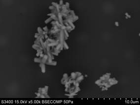
In the case of sol-gel ITO samples, both with 5 and 10 layers, the XRD analysis has highlighted the presence of ITO as the only compound. The crystallinity degree increase with the number of layers, due to the higher number of thermal treatment cycles (as previously observed on the former sol-gel samples). In the case of junction-type samples, ITO5/ZnO and ITO10/ZnO, it can be noticed the specific peak of ZnO and the peak previously assigned to ITO, suggesting a non-uniform and discontinuously covering of the n-type film, which could make I-V measurements improper. By the point of view of ZnO phase, there are differences regarding the (002) peak intensity, placed at 2θ~35°, which is much larger for the sample deposited on ITO5. This fact suggest the different orientation of ZnO nanorods (and so a different growing mechanism) on ITO. For ITO5/ZnO and ITO10/ZnO samples was emphasized the formation of ZnO nanorods (NR) of different sizes – Fig. 1, but in a non-uniform and discontinuous distribution. This fact might be due to the lack of a previous seed layer and could be an explanation for the Hall effect results (Table 15), which are very similar to those made on ITO5 and ITO10.
Fig. 1. SEM images on n/p junction (samples described in Table 1)
Table 15. Hall effect measurements for the films used in n/p junction achievement
6.a.2. Indium Tin Oxide (ITO) and Copper Indium Selenide (CIS) films based junctions
In the second stage (6.1.2) experiments for obtaining solid state semiconductor junctions based on ITO and CIS have been performed. The results are shown for the following type of samples (Table 16).
Table 16. Samples based on Indium Tin Oxide (ITO) and Copper Indium Selenide (CIS) used for obtaining solid state semiconductor junctions
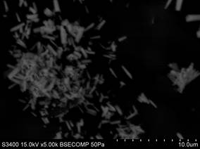
As previously have been determined (stage 6.1.1), ITO films with 5 and 10 layers presents only the crystalline structure of ITO phase and displays continuous and smooth (RMS < 1 nm) layer. XRD investigations highlighted, for the ITO5-CIS and ITO10-CIS, both the specific diffraction lines of CIS – “roquesite” and those previously assigned to ITO, suggesting either the non-uniform and discontinuous covering of the n-type semiconductor film (invalidate by SEM at 500X magnifying), either the reduced thickness of the CIS film. Similar to the ZnO films deposited on ITO, the crystallinity degree of the roquesite phase is higher for the layer deposited on ITO5 than on ITO10. This fact suggests the existence of a different growing mechanism of the CIS film on ITO, depending on the thickness of ITO layer. The CIS film deposited on microscopic glass – reference sample – showed an unique phase of roquesite with a crystallinity degree lower than the sample deposited on ITO5 (due to the amorphous nature of the substrate), but a higher degree than the sample deposited on ITO10 (where growth mechanism problems interfere, as previously mentioned). The
SEM analysis revealed for the reference sample a good covering of the substrate
with a continuous film. Onto its surface spherical micro particles with a
diameter ≤1 µm can be found. A related morphology is found in the case of
ITO5-CIS and ITO10-CIS structures. The size of spherical particles seems to be
slightly lower for ITO10-CIS, possibly due to the presence of centers which
promote The I-V analysis highlighted the resistive behavior of the ITO5-CIS and ITO10-CIS structures. The maximum current value in the -3.5¸3.5 V is higher for ITO10-CIS, possibly due to the higher carrier concentration (identified by Hall effect measurements) and due to a more homogeneous layer. The absence of the diode-type behavior might be due to a number of factors, like: (i) the low ITO film thickness, possibly accompanied by physical shunts (discontinuities) or due to non-stoichiometry; (ii) CIS non-stoichiometry and distribution heterogeneity, due to non-uniform nucleation/ growth processes, correlated to substrate non-homogeneity; (iii) structural non-uniformity in the contact area, due to the too small usefully surface of the samples (when exclude grip and drain areas). Also, by ITO-ITO I-V measurements made before and after masking for CIS layer deposition, defects have been detected. These defects are due to inadequate masking, fact related to the relatively small surface area of the samples.
6.a.3. n-p-n Junctions based on Titanium Dioxide (TiO2), In+N co-doped Zinc Oxide (ZnO:In+N) or Li+Ni (ZnO:Li+Ni) and Al doped Zinc Oxide (AZO) films (AZO)
On the structures dense TiO2 film was deposited by SPD, at a temperature of 350 °C, by masking ½ of each sample. The samples were then thermally treated at 450 °C for 1 hour. The preparation conditions of TiO2 films are summarized in Table 17. The final step after TiO2 film deposition usually involves ethanol sonication of the samples for 30 seconds, to remove powder traces existing on the sample surface, followed by sample drying with compressed air. After this stage, the areas where the TiO2 and p (ZnO) were overlapped, by sonication these layers were removed. The areas were the layers weren’t overlaid remain intact. So, it was noticed that the half of the sample uncovered with TiO2 doesn’t have destruction marks. As a result, the pyrolysis of TiO2 and thermal treatment stages were repeated on the non-damaged surface of the samples, giving up for final sonication of the samples. Subsequent measurements (SEM, EDX, I-V) have been done only on the halves containing all three film types: n-type film (AZO, ITO) / p-type film (INZO, LNZO) / n-type film (TiO2).
Table 17. Samples based on TiO2/ZnO (co-doped)/AZO used for n-p-n semiconductor junction achievement
The SEM analysis revealed that the TiO2 film morphology is not a classical grainy one, possibly due to the powder presence at the film surface (as the high TiO2 percent found by EDX indicates – point analysis). Also, it is possible that the nanorods morphology of the p-type (ZnO) film promotes a disordered growth of the TiO2 film on edges and corners, inducing emphasized roughness/porosity. EDX analysis was used to confirm the presence of the three films involved in n-p-n junction: n-ZnO, p-ZnO and n-TiO2. In this regard, it can be observed (Table17) the significant decrease of the Zn elemental percent from each studied sample. This fact is in the first place due to Zn shielding by Ti from the TiO2 dense film deposited on top; also it cannot be excluded a partial washing of the ZnO film after TiO2 film spraying (due to carrier gas pressure = 1.1 bar, precursor solution composition – water-ethanol, TiCl4, etc). The presence of Ti varies in points, indicating a shallow variable composition of the film and/or its presence as powder at the “sandwich” surface; unfortunately, inability to use the sonication stage made the surface powder removal impossible. One exception is represented by the sample no. 15, for which mapping indicates a limited covering of the ZnO film and so a discontinuous TiO2 film. It is noteworthy that the ZnO amount significantly varies on the surface of the same sample, and on different samples comparatively presented.
Table 18. Percent ratio obtained from superficial mapping of the samples used in n-p-n junctions
Photovoltaic (PV) response. Current – Voltage (I-V) curves
The results of I-V analysis showed a diode behavior in darkness and PV response under irradiation. Based on PV response the characteristic parameters of a photovoltaic cell could be calculated: the short circuit current ISC, the open circuit voltage VOC, the maximum voltage Vmax, the maximum current Imax, the maximum power Pmax, the filling factor FF. The values of these parameters of interest are displayed in Table 19.
Table 19. The characteristic parameters of a PV cell: the short circuit current ISC, the open circuit voltage VOC, the maximum voltage Vmax, the maximum current Imax, the maximum power Pmax and the filling factor FF
The I-V measurements in darkness and under irradiation, demonstrated the achievement of a transparent photovoltaic structure and VIS-active (spectral domain of the irradiation source = UV-NIR). A potential application of these structures could be in glazed surfaces with photo-active properties (for solar energy conversion devices, where the produced energy can be used in defroster, or for building windows). Although the values of Imax, Vmax, ISC, VOC are significantly lower than those of the traditional PV structures (with dyed p-semiconductor), the filling factor of the studied samples is promising, of about 24 – 25 %. The maximum value of the filling factor is found for sample no. 10 (which has the most uniform morphology compared to the rest of the samples). Thus, the structures of samples 11 and 14 could be taken into consideration for a later study (optimization), each of them containing ZnO based homojunctions. From electrical measurements, but also from previous structural and morphological analyses, it was observed that ITO-ZnO heterojunctions lead to lower electrical properties compared to homojunctions, due to film interface recombinations and due to reduced thickness of ITO films or its non-homogeneity (stages 1.1 and 1.2).
6.b. Laboratory tests of DSSC solar cell configuration
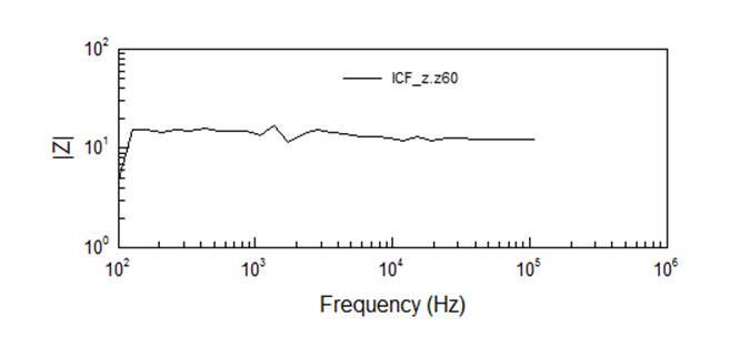
Dye-sensitized solar cells (DSSC) are part of the third generation of solar cells, and could be considered at the beginning of their development cycle because it is expected to have an intensive evolution in the next period, due to their certain advantages in relation to other solar cells: they have low production costs, involves well-established fabrication technologies (serigraphy, rotary printing, etc), the highest conversion yield in low lighting conditions (clouded sky or interior light sources), the conversion yield increase when the cell temperature increase (at Si-based solar cells the conversion yield drops when the temperature increase), etc. The transparent and conductive layers specimens obtained in the frame of the present project proved to be compatible with the technological flow of dye-sensitized solar cells (DSSC) prototypes achievement. The obtained transparent and conductive electrodes retain its electrical properties after the thermal treatments (max. 550 °C) and form a stable interface, with low impedance, as it can be seen form the impedance spectrum of a dye-sensitized solar cell, with a conductive and transparent ZnO layer (Fig. 2). The optical transmission of these electrodes exceeds 80% in the spectral range of 350 – 800 nm.
Fig. 2. Impedance spectrum of a dye-sensitized solar cell, obtained with a ZnO based transparent conductive electrode
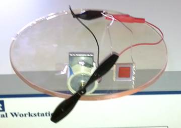
A number of 14 prototypes of dye-sensitized solar cells (DSSC) have been achieved, for which a 10 years lifetime is expected. In Fig. 3 is presented an example of such a cell, which powers a micro-engine (ending with a propeller), while in Table 20 are summarized the best 3 results obtained.
Table 20. Details about the synthesis and properties of the best DSSC-type cells achieved in the frame of the project
The generated voltage by the solar cells based on transparent and conductive electrodes achieved in the frame of this project has similar values with those obtained on Pilkington (USA) reference electrode, under the same irradiation conditions. The short-circuit current of these cells is about 3–5 mA/cm2. By using an acetonitrile-based electrolyte, the short-circuit current significantly increases (it doubles), but the use of this type of electrolyte has the disadvantage of solvent lose out by evaporation.
Potential applications:
These types of solar cells can have a multitude of application, among which we mention: - the powering of sensors and transmitters (measurement of temperature, humidity, presence / absence indicators, etc) placed inside and outside the buildings; - the powering of different systems used in IoT (“internet of things”); - the powering of different mobile systems (mobile phones, measurement and control equipment, etc).
Free website templates |
|||||||||||||||||||||||||||||||||||||||||||||||||||||||||||||||||||||||||||||||||||||||||||||||||||||||||||||||||||||||||||||||||||||||||||||||||||||||||||||||||||||||||||||||||||||||||||||||||||||||||||||||||||||||||||||||||||||||||||||||||||||||||||||||||||||||||||||||||||||||||||||||||||||||||||||||||||||||||||||||||||||||||||||||||||||||||||||||||||||||||||||||||||||||||||||||||||||||||||||||||||||||||||||||||||||||||||||||||||||||||||||||||||||||||||||||||||||||||||||||||||||||||||||||||||||||||||||||||||||||||||||||||||||||||||||||||||||||||||||||||||||||||||||||||||||||||||||||||||||||||||||||||||||||||||||||||||||||||||||||